Understanding the Different Types of PCBs: Single, Double, and Multilayer Boards
Printed Circuit Boards (PCBs) are the foundational building blocks of most electronic devices, serving as the framework that connects and supports various components such as resistors, capacitors, and integrated circuits. Depending on the application, PCBs can vary in complexity, design, and materials. Broadly speaking, they fall into three primary types: single-layer, double-layer, and multilayer boards. Each type of PCB offers unique advantages and trade-offs that impact design, manufacturing, and end-use performance. In this article, we’ll delve into the characteristics, applications, and benefits of these PCB types.
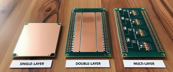
1. Single-Layer PCBs
Description:
Single-layer or single-sided PCBs are the simplest type of PCB, featuring a single conductive layer. The conductive material, typically copper, is applied to one side of the base material (substrate), which can be made of FR4, a glass-reinforced epoxy laminate, or other insulating materials. Components are mounted on one side of the board, with the conductive traces running on the opposite side.
Advantages:
• Cost-Effectiveness: Single-layer boards are the least expensive to produce, as they require fewer materials and simpler manufacturing processes.
• Ease of Design and Manufacture: Due to their simplicity, single-layer PCBs are easy to design and manufacture, making them ideal for prototyping.
• Reliability: With only one layer of copper and a straightforward layout, single-layer boards are generally less prone to defects.
Applications:
• Consumer Electronics: Single-layer PCBs are commonly used in low-cost, high-volume products like calculators, remote controls, and toys.
• Power Supplies: Their basic structure suits applications where complex circuitry isn’t necessary, such as power distribution and LED lighting.
• Household Appliances: Single-layer boards often power simple, single-function appliances like coffee makers and washing machines.
2. Double-Layer PCBs
Description:
Double-layer or double-sided PCBs have two conductive layers, one on each side of the substrate. Components can be mounted on both sides, which allows for increased circuit density. Double-layer boards also incorporate vias (small holes filled or plated with conductive material) that connect the two layers, enabling more complex circuits than single-layer PCBs.
Advantages:
• Greater Circuit Density: With two conductive layers, double-sided PCBs can support more components and connections, making them suitable for more sophisticated applications.
• Enhanced Flexibility in Design: Designers have more options to route traces and interconnect components, which can help minimize the overall size of the PCB.
• Balanced Cost and Complexity: Double-layer PCBs offer a good balance between cost and performance, making them popular for medium-complexity applications.
Applications:
• Industrial Controls: Double-layer PCBs are often used in industrial control systems where moderate circuit complexity is required.
• Automotive Electronics: Automotive systems like sensors and dashboard electronics utilize double-layer boards for their moderate complexity and durability.
• Power Conversion: These boards are common in converters, power controllers, and other moderate-complexity power systems.
3. Multilayer PCBs
Description:
Multilayer PCBs consist of three or more conductive layers, separated by insulating layers, and are laminated together under high pressure and temperature. This layering allows for highly compact and complex designs with significantly higher component density. Multilayer boards are often built with an odd number of layers, which helps reduce warping during the manufacturing process. With internal layers for power and ground planes, multilayer PCBs offer superior electrical performance, especially in high-speed circuits.
Advantages:
• High Component Density: Multilayer boards support advanced designs with a large number of components, which is ideal for miniaturized devices.
• Improved Signal Integrity: By dedicating inner layers to power and ground planes, multilayer PCBs reduce electromagnetic interference (EMI), improving signal quality.
• Enhanced Durability and Reliability: The lamination process used in multilayer PCBs makes them durable, with good resistance to external conditions.
Applications:
• Consumer Electronics: High-performance devices like smartphones, laptops, and wearables rely on multilayer boards for their compact designs and high functionality.
• Telecommunications: Multilayer PCBs are used in routers, switches, and other telecom equipment that require fast signal processing and complex circuitry.
• Medical Devices: Devices such as heart monitors and imaging equipment use multilayer boards for their compact size, reliability, and signal integrity.
________________________________________
| PCB Type | Layers | Complexity | Cost | Common Applications |
| Single-Layer | 1 | Low | Low | Power Supplies |
| Double-Layer | 2 | Medium | Moderate | Automotive, Industrial Controls |
| Multilayer | 3+ | High | High | Smartphones,Medical Devices, Telecom |
Choosing the Right PCB Type:
Selecting the appropriate PCB type depends largely on the specific application requirements, budget, and design complexity. Single-layer PCBs are sufficient for simple, low-cost electronics, while double-layer PCBs offer moderate complexity and performance, balancing cost and functionality. Multilayer boards are essential in advanced applications where compact size, high signal integrity, and reliability are paramount.
Understanding the differences between single, double, and multilayer PCBs is crucial for electronics engineers, product designers, and manufacturers. The right PCB type can dramatically impact the performance, durability, and cost-efficiency of the final product. By aligning PCB selection with application requirements, engineers can optimize their designs for performance, cost, and ease of manufacture, helping to create reliable and high-performing electronics across industries.