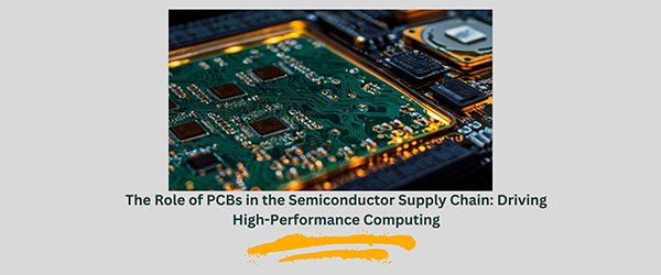
The Role of PCBs in the Semiconductor Supply Chain: Driving High-Performance Computing
Printed Circuit Boards (PCBs) are the backbone of modern electronic devices, serving as the platform for integrating semiconductors and enabling their functionality. As technology advances, the relationship between PCBs and the semiconductor industry becomes increasingly critical. This article explores how innovations in the semiconductor supply chain shape PCB designs, their manufacturing complexities, and their impact on high-performance computing (HPC).
Semiconductors and PCBs: A Symbiotic Relationship
Semiconductors are the brains of modern electronics, while PCBs are the nervous system that connects and powers them. The interplay between these two components is vital for developing cutting-edge technologies in industries such as telecommunications, automotive, aerospace, and consumer electronics.
The rise of advanced semiconductors—like system-on-chip (SoC) designs and multi-die architectures—demands equally sophisticated PCBs. These boards must accommodate higher speeds, lower power consumption, and greater reliability while managing the heat generated by these high-performance chips.
Key Challenges in PCB Design for HPC Applications
1. High-Density Interconnection (HDI)
HDI PCBs are essential for integrating complex semiconductors. These boards have finer lines, smaller vias, and higher layer counts, enabling compact designs without sacrificing functionality.
Feature | Traditional PCB | HDI PCB |
Trace Width | >100 µm | <50 µm |
Layer Count | <10 | 10–30+ |
Via Technology | Through-hole | Micro-via/Blind Via |
2. Signal Integrity and High-Speed Design
Modern HPC systems operate at frequencies exceeding 1 GHz, requiring PCBs that minimize signal loss and interference. Designers use controlled impedance, low-loss materials, and differential pair routing to ensure performance.
Key Requirements for Signal Integrity:
- Dielectric Material: Low dielectric constant (Dk) and dissipation factor (Df).
- Trace Design: Consistent impedance matching for high-speed signals.
3. Power Integrity and Thermal Management
High-performance semiconductors demand efficient power delivery and robust thermal dissipation to avoid overheating and ensure reliability. Solutions include:
- Power Distribution Networks (PDNs): Optimize layer stacks to reduce resistance and inductance.
- Thermal Via Arrays: Conduct heat away from hot spots.
- Embedded Heat Sinks: Direct heat to dissipative materials.
Impact of Semiconductor Trends on PCB Development
Trend 1: Chiplet Architectures
Chiplets integrate multiple small dies into a single package, enhancing performance while reducing cost. PCBs must support advanced interconnect technologies like high-bandwidth memory (HBM) and heterogeneous integration.
Aspect | Traditional Chips | Chiplets |
Interconnect | Solder balls | High-density routing |
Power Delivery | Standard PDNs | Ultra-low noise PDNs |
Trend 2: 3D Packaging
Semiconductor manufacturers are shifting toward 3D packaging, which stacks chips vertically to save space. This necessitates PCBs with ultra-thin traces and advanced materials to manage the additional heat and signal complexity.
Examples of 3D Packaging Impacts:
- Routing Complexity: Denser via structures.
- Thermal Design: Enhanced cooling layers.
Trend 3: Transition to AI and Machine Learning
AI chips like TPUs and GPUs require extreme bandwidth and low latency, pushing PCBs to new limits in terms of signal integrity and power efficiency.
Challenge | AI-Driven Requirement |
Data Bandwidth | High-speed serial links |
Latency | Reduced propagation delay |
Thermal Management | Superior heat dissipation |
Advanced Manufacturing Techniques
To meet these demands, PCB manufacturers are adopting innovative techniques, such as:
- Laser-Drilled Microvias: Ensures precise connections for HDI designs.
- Embedded Passive Components: Reduces board space and improves performance.
- Automated Optical Inspection (AOI): Detects defects in complex PCBs.
Future Outlook
The PCB industry will continue to evolve alongside semiconductor advancements. Key focus areas include:
- Integration of Optical Interconnects: For ultra-high-speed communication.
- Development of Biodegradable PCBs: For sustainability.
- AI-Enhanced PCB Design Tools: To optimize layouts for new-generation semiconductors.
The collaboration between PCB and semiconductor industries is more critical than ever. By aligning innovation in both sectors, the promise of high-performance computing can be fully realized, powering the next wave of technological breakthroughs.