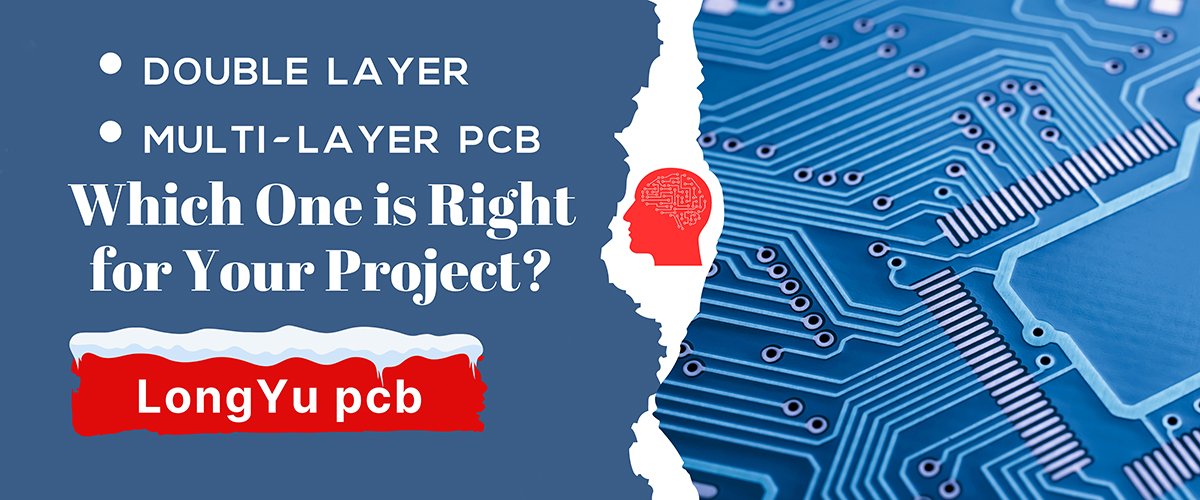
In the world of electronics, choosing the right type of printed circuit board (PCB) is crucial for the performance, cost-effectiveness, and reliability of your product. PCBs come in various forms, but the most common types are double-layer and multi-layer PCBs. Understanding the differences between them will help you make an informed decision based on your specific needs.
This article will provide a detailed comparison of double-layer and multi-layer PCBs, highlight their advantages and disadvantages, and include helpful tables for easy comparison. We’ll also include SEO keywords like "double layer PCB," "multi layer PCB," "PCB comparison," "PCB design," and "multi layer PCB advantages."
What is a Double-Layer PCB?
A double-layer PCB is a type of printed circuit board that has two conductive layers. These layers are connected through vias (small holes that pass through the PCB and connect the two sides). This design allows for a more compact layout and is often used in applications where space is limited but more than one layer of components or circuitry is needed.
Features of Double-Layer PCBs:
What is a Multi-Layer PCB?
A multi-layer PCB is a more advanced version of a double-layer PCB. It consists of three or more conductive layers that are stacked together. These layers are also interconnected through vias, but the process is more complex due to the increased number of layers.
Features of Multi-Layer PCBs:
- --- More than two conductive layers (typically 4, 6, or more).
- --- The layers are interspersed with insulating layers.
- --- Offers higher performance and density for complex circuits.
Key Differences Between Double-Layer and Multi-Layer PCBs
To help you understand the differences more clearly, here’s a detailed comparison of double-layer and multi-layer PCBs in terms of their features, advantages, disadvantages, and applications.
Feature | Double-Layer PCB | Multi-Layer PCB |
Number of Layers | 2 (two conductive layers) | 3 or more layers (commonly 4, 6, or 8 layers) |
Size and Complexity | Simpler design, compact and less complex | More complex and dense design |
Manufacturing Cost | Lower cost | Higher cost due to more materials and labor |
Signal Integrity | Moderate signal integrity | Higher signal integrity, especially for high-speed signals |
Circuit Density | Medium (can handle medium-density circuits) | High (can handle complex, high-density circuits) |
Design Flexibility | Less flexibility compared to multi-layer | High flexibility for complex designs |
Applications | Used in low-to-medium complexity applications | Used in high-complexity, high-performance electronics like computers, telecommunications, and medical devices |
Board Thickness | Typically thinner compared to multi-layer PCBs | Thicker and bulkier due to multiple layers |
Heat Dissipation | Moderate heat dissipation | Better heat dissipation due to multiple layers and better routing options |
Electrical Performance | Good for low-to-medium frequency circuits | Excellent for high-frequency, high-performance circuits |
Manufacturing Time | Faster production time | Longer production time due to the complexity of design |
Advantages of Double-Layer PCBs:
--- Cost-Effective: Double-layer PCBs are less expensive to manufacture compared to multi-layer PCBs.
--- Compact Design: With two conductive layers, they are smaller and more suitable for devices where space is a constraint.
--- Simplicity: Easier to design and faster to manufacture, making them ideal for simpler applications.
--- Good for Low-to-Medium Complexity: Double-layer PCBs are perfect for basic devices like consumer electronics, power supplies, and basic communication equipment.
Advantages of Multi-Layer PCBs:
--- High-Density Circuits: Multi-layer PCBs can handle much more complex circuits with higher functionality, which is ideal for high-performance devices.
--- Improved Signal Integrity: The extra layers help reduce signal loss, making multi-layer PCBs more suitable for high-speed communication systems.
Compact Design for Complex Circuits: Despite their higher layer count, multi-layer PCBs allow for a compact design, making them ideal for modern, miniaturized devices.
- --- Superior Heat Dissipation: Multi-layer PCBs offer better heat dissipation compared to double-layer PCBs, ensuring that the components do not overheat.
--- Better Electrical Performance: Multi-layer PCBs provide better electrical performance, particularly for high-frequency applications.
Disadvantages of Double-Layer PCBs:
- --- Limited Circuit Density: Since it only has two layers, the available space for routing is limited, which might not be sufficient for more complex designs.
--- Signal Integrity: While good for basic applications, double-layer PCBs can suffer from signal loss and integrity issues at higher frequencies.
Disadvantages of Multi-Layer PCBs:
- --- Higher Cost: Due to the complexity of manufacturing and the use of more materials, multi-layer PCBs are more expensive than double-layer PCBs.
- --- Longer Production Time: Multi-layer PCBs take more time to design and manufacture due to their intricate design and additional layers.
- --- More Complex Design: The complexity of routing multiple layers requires specialized knowledge, making the design process more difficult.
Choosing Between Double-Layer and Multi-Layer PCBs:
When selecting the right type of PCB for your project, you need to consider the following factors:
- --- Project Complexity: If your design requires a high-density circuit with multiple components and signals, a multi-layer PCB is the better choice.
- --- Size and Space Constraints: If you need a more compact design but don’t require too many layers, a double-layer PCB will suit your needs.
- --- Cost: If you're working on a budget and the design complexity is low, double-layer PCBs offer an affordable solution.
--- Performance: If your product requires high-speed data transfer or operates in an environment with high-frequency signals, multi-layer PCBs offer better performance and signal integrity.
Common Applications of Double-Layer and Multi-Layer PCBs
Application | Double-Layer PCB | Multi-Layer PCB |
Consumer Electronics | Smartphones, digital cameras, gaming consoles | High-end smartphones, laptops, tablets |
Automotive Electronics | Sensors, basic control units | Advanced navigation, infotainment systems |
Telecommunications | Simple network devices | Routers, base stations, data centers |
Medical Devices | Basic diagnostic equipment | Complex medical imaging and diagnostic devices |
Industrial Equipment | Control boards, power supplies | Automated systems, robotics, CNC machines |
Both double-layer PCBs and multi-layer PCBs offer distinct advantages depending on the complexity and requirements of your project. While double-layer PCBs are a cost-effective solution for less complex applications, multi-layer PCBs are designed for more sophisticated circuits, providing higher density, better performance, and superior signal integrity.
If you are looking for a PCB that can handle complex and high-performance applications, a multi-layer PCB might be the best choice. However, if you're on a budget or working on a simpler design, a double-layer PCB will be more than sufficient.
By carefully considering your project’s needs, you can choose the ideal PCB that offers the right balance of performance, cost, and reliability.