
Double Layer PCB
Double-Layer PCB
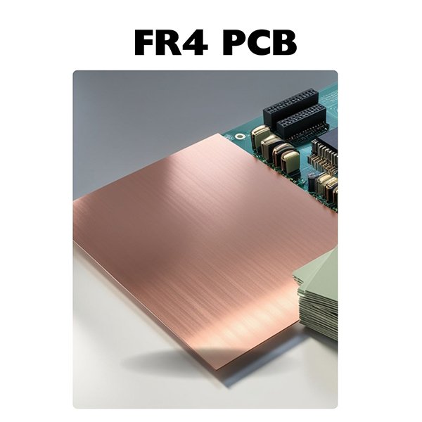
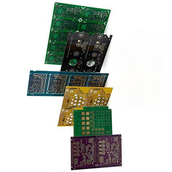
A Double-Layer PCB, also known as a two-layer PCB, is an advanced circuit board featuring two layers of conductive copper, allowing connections on both the top and bottom layers. This design offers enhanced routing capacity compared to single-layer PCBs, making it ideal for more complex circuits that require compact layouts. Double-layer PCBs are widely used in applications such as industrial controls, automotive electronics, consumer devices, and communication equipment. With our quality materials and precision manufacturing, these PCBs ensure durability, performance, and reliability for various electronic projects.
Key Features:
--- Increased Circuit Density: Maximizes board space and accommodates complex circuit layouts.
--- Efficient Design: Supports higher functionality within a smaller footprint.
--- Cost-Effective: Offers a balance between complexity and cost, suitable for a wide range of applications.
--- Versatility: Applicable for both analog and digital circuits.
Technical Specifications:
| Specification | Description |
| Layers | 2 |
| Base Material | FR-4, CEM-3, or requested material |
| Board Thickness | Standard: 1.6 mm (Customizable) |
| Copper Thickness | 1 oz (35 µm), customizable upon request |
| Min Trace Width | 0.15 mm |
| Min Trace Spacing | 0.15 mm |
| Surface Finish | HASL, ENIG, OSP, or custom finish |
| Solder Mask Color | Green (Other colors available) |
| Drill Hole Size | Minimum 0.3 mm |
| Impedance Control | Available |
| Operating Temperature | Up to 130°C |
Applications:
--- Consumer Electronics
--- Automotive Systems
--- Industrial Controls
--- Communication Devices
--- Medical Equipment
Contact Us to learn more about how our double-layer PCBs can meet your project requirements, or to request a customized solution.