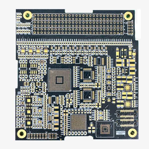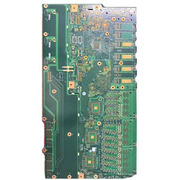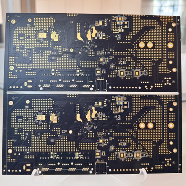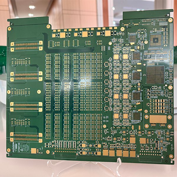

8L Microwave PCB Isola Astra MT77
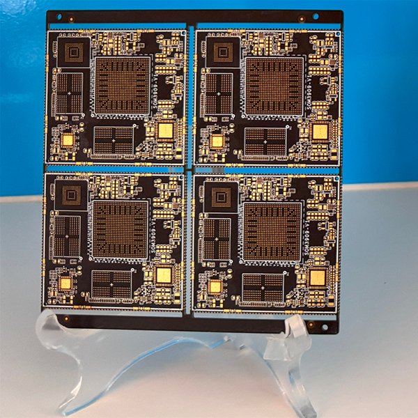
8L Microwave PCB Isola Astra MT77
Overview
Microwave printed circuit boards (PCBs) are specialized substrates optimized for use at microwave frequencies, typically defined as signals exceeding 1 GHz. This technology plays a crucial role in facilitating high-frequency wireless communications, radar systems, electronic warfare, and testing equipment, operating effectively at millimeter wave frequencies up to 100 GHz.
Benefits of Microwave Printed Circuit Boards:
Utilization of Low-CTE Materials: These materials help stabilize PCBs in high-temperature conditions.
Flawless Layer Alignment: Ensures a smooth and precise alignment of various layers.
Alignment of Multiple Layers: Low CTE materials facilitate the alignment of numerous layers within intricate structures.
Reduced Assembly Costs: Helps lower overall production expenses.
Enhanced Performance: Delivers optimal functionality.
Better High-Frequency Signal Transmission: Improves the efficiency of signal transmission at high frequencies.
Supports More Complex Designs: Allows for the creation of intricate and sophisticated designs.
Microwave PCB Fabrication and Assembly:
The creation of microwave printed circuit boards involves sophisticated manufacturing techniques and assembly methods:
Material Evaluation: Properties such as dielectric constant and loss tangent are thoroughly assessed on production panels to ensure quality.
Surface Treatment: Oxide treatments and chemical preparations are employed to improve copper adhesion.
Etching Techniques: Conductors are formed using printed, plated, or etched methods to achieve intricate designs with smooth contours.
Layer Alignment: Precise alignment during layer stacking and lamination minimizes parasitic effects.
Hole Quality Assurance: Drilling techniques ensure high-quality hole walls for dependable plated via connections.
Solder Mask Application: A photoimageable mask offers excellent spatial accuracy for enhanced component placement.
Pad and Gap Specifications: Conductor layouts are precisely matched to chip terminations within micrometer tolerances.
Plating Supervision: Stringent control over plating thickness and hole filling maintains consistent electrical performance.
Automated Evaluation: Comprehensive electrical testing verifies impedance, signal propagation, and resonant frequencies.
Controlled Assembly Processes: Surface Mount Technology (SMT), wire bonding, and conformal coating are executed according to established protocols.